Electrical Engineering
The Theory of the Vacuum Tube and Its Relation to the JFET
This chapter provides a brief overview of the theory from vacuum tubes to MOSFET transistors. It does not include the full derivation of all the formulas or the complete physics of the devices.
1. Historical Introduction
Long before transistors revolutionized electronics, the vacuum tube was the heart of all amplifiers, oscillators, and radio transmitters. In the early 20th century, pioneers such as Lee de Forest (with his triode, 1906) developed a technology that enabled wireless communication and laid the foundations of modern electronics. Tubes were found in the first radios, early computers like the ENIAC, and nearly every electronic device until the 1950s. The invention of the transistor in 1947 marked the beginning of the vacuum tube's decline, but in specialized fields like audio amplification and high-frequency technology, it remains highly regarded. Interestingly, many principles of vacuum tube technology reappear in modern semiconductor components, especially in the JFET (Junction Field Effect Transistor), whose operation closely resembles that of the triode.
2. Basic Operation Principles
Vacuum Tube (Triode): A triode consists of a cathode, a control grid, and an anode. The anode current \(I_a\) depends on grid voltage \(V_g\) and anode voltage \(V_a\).
JFET (n-channel): An n-channel JFET has source, drain, and gate. The drain current \(I_D\) is controlled by \(V_{GS}\).
3. Mathematical Description
Triode:
\[I_a = k \cdot \left(V_g + \frac{V_a}{\mu}\right)^{3/2}\tag{1}\]
JFET:
\[I_D = I_{DSS} \left(1 - \frac{V_{GS}}{V_P}\right)^2\tag{2}\]
4. Analogy between Triode and JFET
Both devices modulate current via a control voltage:
- JFET: quadratic dependence
- Triode: 3/2 power law
5. Deriving the Tube Equation from Space-Charge Theory
\[I_a = \frac{4 \varepsilon_0}{9} \sqrt{\frac{2e}{m}} \cdot \frac{A}{d^2} V_a^{3/2}\tag{3}\]
With effective potential:
\[V_{eff} = V_g + \frac{V_a}{\mu}\Rightarrow I_a = k \cdot \left(V_g + \frac{V_a}{\mu}\right)^{3/2}\tag{4}\]
6. Conclusion
The vacuum tube is a historical key to understanding modern analog electronics. Its principles live on in field-effect transistors such as the JFET.
From Bipolar Transistors to CMOS Technology
1. The Transition from Tubes to Semiconductors
The invention of the transistor by John Bardeen, Walter Brattain, and William Shockley at Bell Labs in 1947 marked a fundamental shift in electronics. Unlike vacuum tubes, which rely on thermionic emission and vacuum-based electron flow, transistors are solid-state devices made from semiconductor materials like silicon and germanium. This shift not only allowed for greater miniaturization and lower power consumption but also significantly improved reliability and opened the door to mass production.
The first widely used transistors were bipolar junction transistors (BJTs), which, like triodes, were used for amplification. However, transistors eliminated the warm-up time, fragility, and high operating voltages associated with vacuum tubes. With their smaller size and compatibility with printed circuit boards, transistors soon found their way into radios, televisions, and the first generation of computers.
As the demand for more complex circuits grew, so did the need for even more compact, energy-efficient, and scalable technologies—leading to the development of integrated circuits (ICs) and ultimately to MOSFET-based designs, which form the backbone of modern digital electronics.
2. From BJT to FET
The transition from BJTs to Field-Effect Transistors (FETs) represented a significant advancement in semiconductor technology. While BJTs are current-controlled devices—requiring a continuous base current to regulate collector current—FETs are voltage-controlled. This key difference results in much lower power consumption for FETs, especially in digital switching applications.
A common early form of the FET is the JFET (Junction Field-Effect Transistor), in which a voltage applied to the gate creates a depletion region that modulates the conductivity of a semiconductor channel between source and drain.
The most widely used type of FET today is the MOSFET (Metal-Oxide-Semiconductor Field-Effect Transistor). In MOSFETs, the gate is electrically isolated from the channel by a thin oxide layer, allowing even better input impedance and lower gate current. MOSFETs can be fabricated in very small dimensions and used in complementary pairs (nMOS and pMOS) to form CMOS logic.
The advantages of FETs—especially MOSFETs—include:
- Extremely low input current
- High switching speed
- Compatibility with high-density integration
3. CMOS: Complementary MOS
Using both NMOS and PMOS transistors, CMOS minimizes power by only consuming energy during switching.
| Input \(V_{in}\) | NMOS | PMOS | Output \(V_{out}\) |
|---|---|---|---|
| 0 V | off | on | \(V_{DD}\) |
| \(V_{DD}\) | on | off | 0 V |
4. Large and Small Signal Behavior
Large Signal Models
BJT:\[ I_C = I_S \cdot e^{\frac{V_{BE}}{V_T}}\tag{5}\]
MOSFET:\[ I_D = \frac{1}{2} k' \cdot \frac{W}{L} \cdot (V_{GS} - V_{th})^2\tag{6}\]
Small Signal Models
- BJT:\[ g_m = \frac{I_C}{V_T}, \quad r_\pi = \frac{\beta}{g_m}\tag{7}\]
- MOSFET:\[ g_m = \frac{2 I_D}{V_{ov}}, \quad g_{ds} \approx \lambda I_D\tag{8}\]
Modeled as:
BJT: \(i_c = g_m v_{be}\tag{9}\)
MOSFET: \(i_d = g_m v_{gs}\tag{10}\)
Summary Table
| Aspect | Large Signal | Small Signal |
|---|---|---|
| Purpose | Switching (DC) | Amplification (AC) |
| Nature | Nonlinear | Linear (around bias) |
| Dependence | Absolute voltage | Small variations |
| Modeling | Full equations | With \(g_m\), \(r_o\) |
5. Conclusion
From vacuum tubes to BJTs and CMOS, electronics evolved in efficiency and complexity. Core analog principles remain the same—only their physical realization has changed.
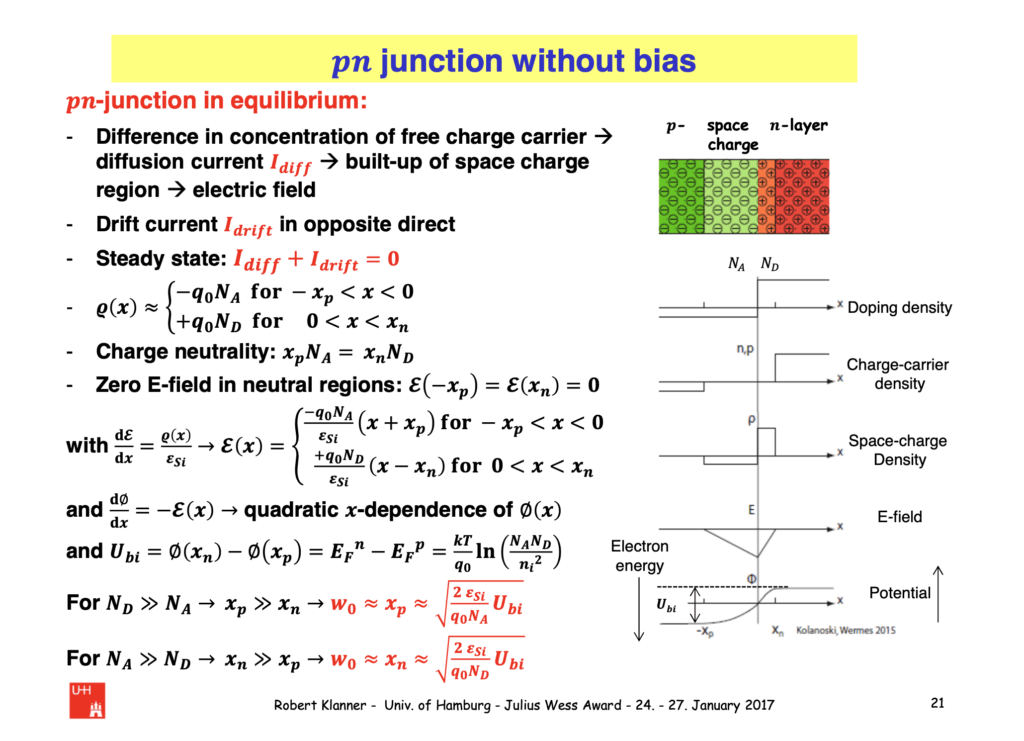
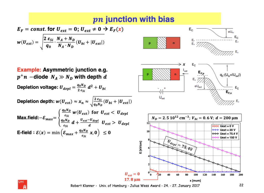
The pn Junction
This chapter provides an overview of the PN junction theory. It does not include the full derivation of all formulas or a complete treatment of the underlying physics. The following descriptions are based on slides from a lecture given by Prof. Dr. Robert Klanner on Silicon Detectors: Concepts, Understanding, and Characterization.